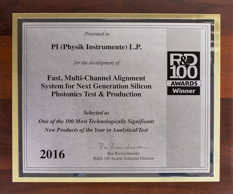
Industry-leading speed and capability is an enabler for “photonomics” from wafer to packaged device; 2016 R&D 100 award winner!
Problem
The convergence of photonics and semiconductors promises a leap in data throughput, parallelism and energy efficiency. Design and materials challenges have by now been addressed. Practicalities of testing and packaging have not.
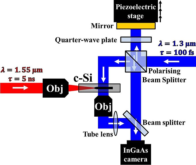
Test and packaging of silicon photonics elements require nanoscale alignments that cannot be performed using visual or mechanical references. Instead, these optimizations must optimize the optical throughput itself. In addition, SiP designs often incorporate multiple parallel optical paths with multiple, interacting inputs and outputs, all needing optimization. Simple economics as well as optical realities dictate that these be optimized simultaneously, yet until now there has been no technology capable of doing this.
Solution
Physik Instrumente (PI) has been the global leader in ultraprecision motion control for semiconductor manufacturing for more than three decades.
Now PI has addressed the need for fast, parallel, nanoscale-accurate, multi-DOF global optical alignment optimization required in key SiP production steps from planar test to packaging.
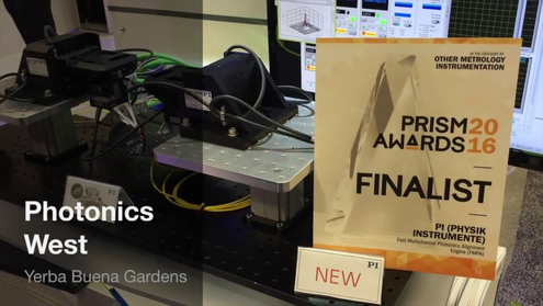
In acknowledgment of this achievement’s importance, the system has been named a 2016 R&D 100 award winner, as one of the 100 most technologically significant products of the year in the Analytical/Test category and a finalist for a 2016 Photonics PRISM award – “The Oscars of Photonics”.
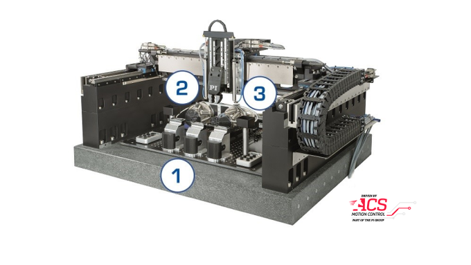
This enabling solution integrates PI’s high-throughput piezo nanopositioning technologies and ultraprecision motion control with novel algorithms. The groundbreaking technology was developed by PI’s team that comprises more than a century of photonics alignment automation experience and includes foundational participants in the field. The system is part of PI’s broad offering of photonics alignment engines ranging from software-driven stage solutions to integrated 6-DOF hexapods with built-in alignment functionality.
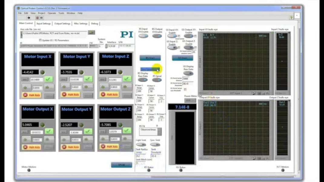
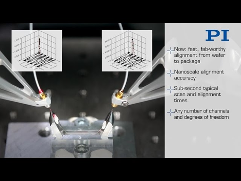
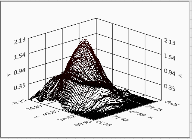
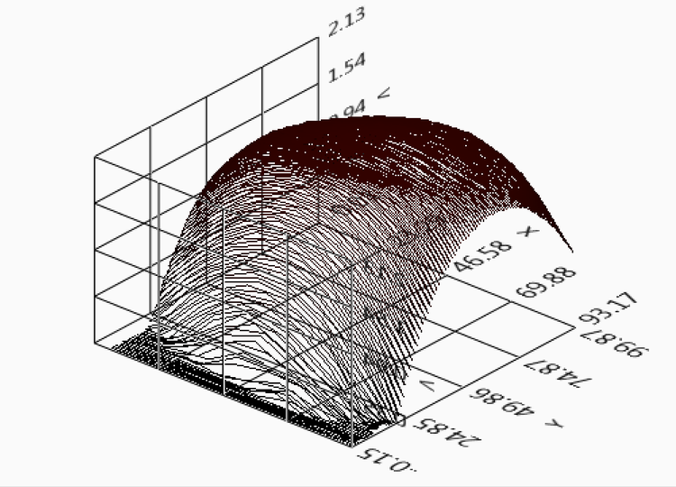
In the video above, first, full-field (100×100 micron) profiling achieves first light—fast. This example application then allows the user to severely de-align the couplings by dragging the mouse, and then recover them in an instant. Finally, a global optimization is achieved by simultaneous gradient searches.
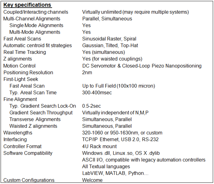
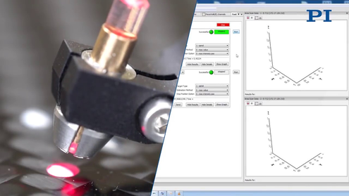
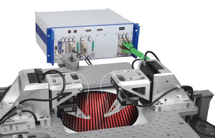
This video (above) shows PI’s new FMPA F-712 system. In this demo, an in-wafer, grating-coupled waveguide device is simulated by a short length of single-mode fiber. Its input and output are coupled via lensed fibers mounted on grippers on PI’s Nanocube XYZ piezo positioner / scanner, which is controlled by the F-712’s controller.
